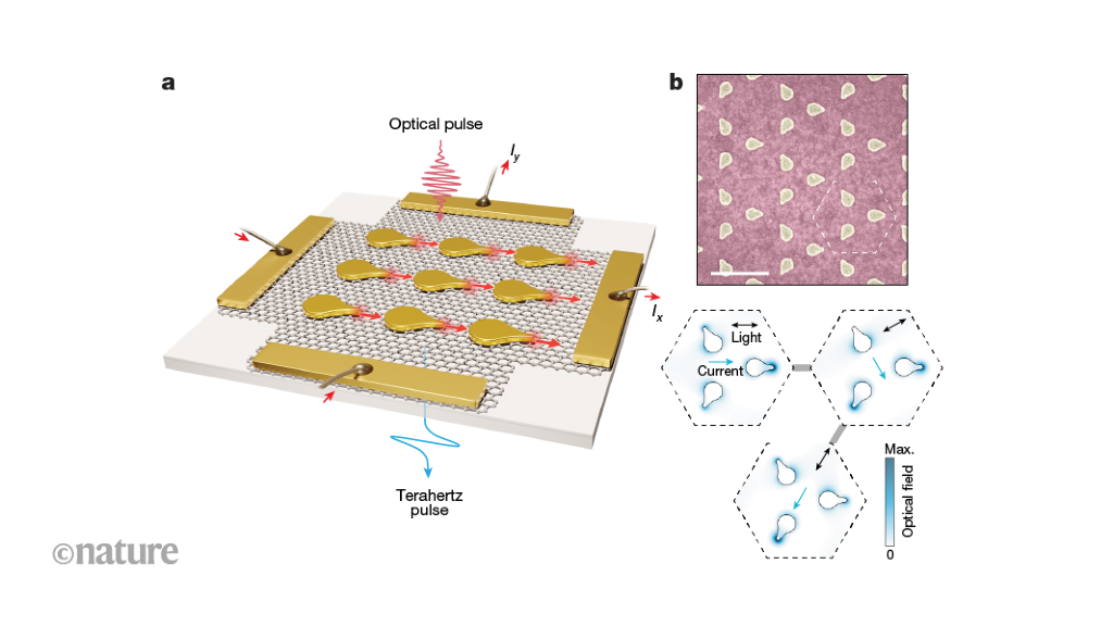
"Light-Powered Nanoscale Control of Electrical Currents for Next-Gen Tech"
Researchers have developed an innovative class of optoelectronic metasurface that allows for precise control of electrical currents at the nanoscale using light. This breakthrough could lead to applications in terahertz science, information processing, and other fields, offering opportunities for ultrafast light-controlled charge flows.