Harvard researchers have developed a novel ultra-thin metasurface that simplifies quantum operations by replacing multiple optical components, potentially revolutionizing quantum computing, sensing, and networking with more scalable, stable, and cost-effective devices.
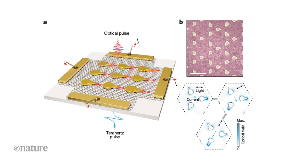
Researchers have developed an innovative class of optoelectronic metasurface that allows for precise control of electrical currents at the nanoscale using light. This breakthrough could lead to applications in terahertz science, information processing, and other fields, offering opportunities for ultrafast light-controlled charge flows.
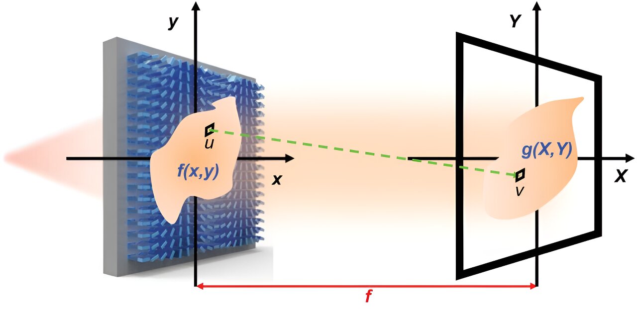
Researchers at Penn State have developed a metasurface, an optical element that mimics the image processing capabilities of the human eye, allowing for instantaneous image transformation before digitalization by a camera. This innovation has the potential to significantly reduce the computing power and energy required for artificial intelligence systems to process images and identify objects, making it easier to recognize objects across different scales and orientations. The metasurface works using nanostructures to bend light and can be applied in various fields, including target tracking, surveillance, and satellite imaging.
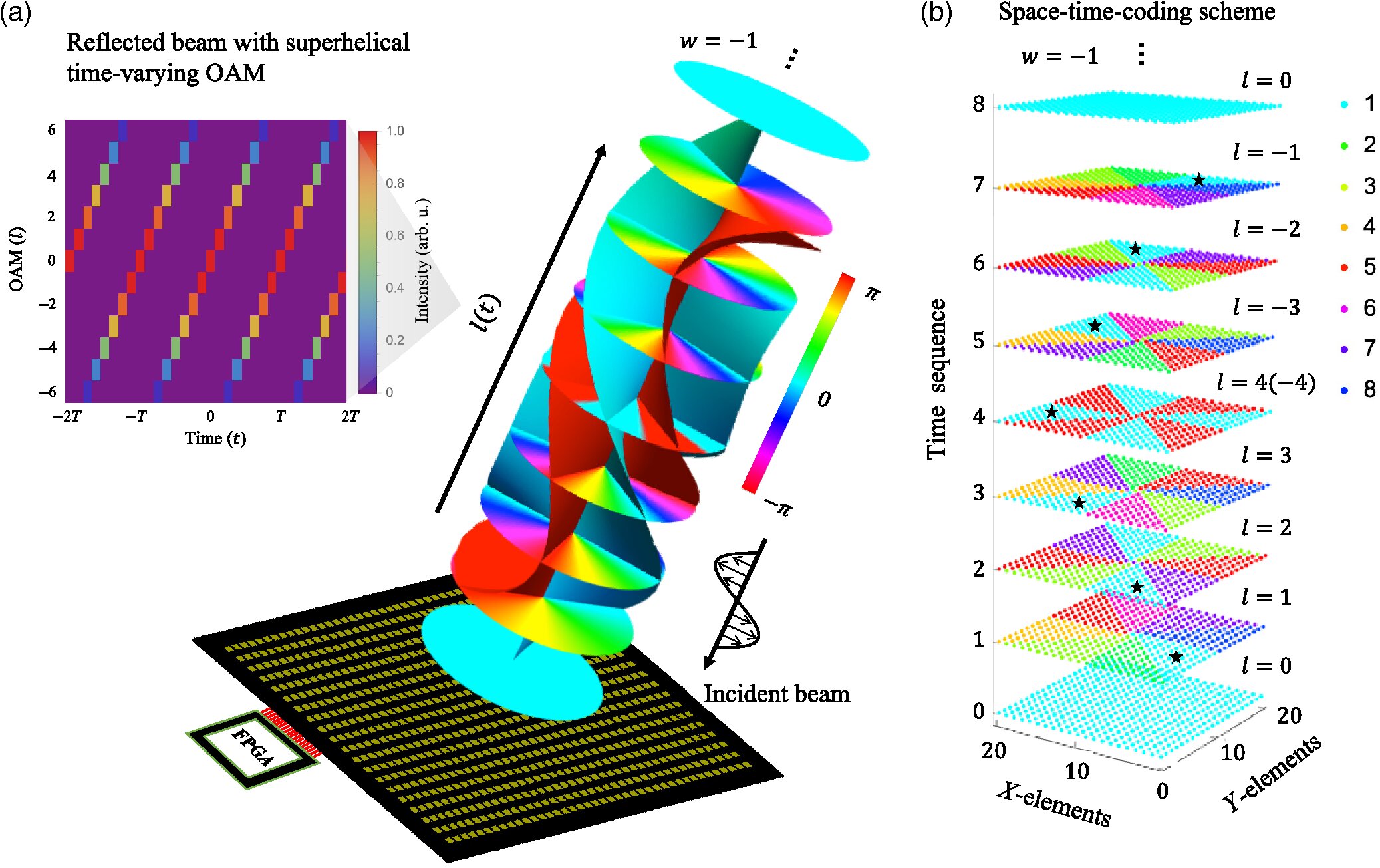
Researchers from The Hong Kong University of Science and Technology and City University of Hong Kong have developed time-varying orbital angular momentum (OAM) beams using a space-time encoded digital metasurface. By exploiting the flexible programmability of the metasurface, they construct different modes of the time-varying OAM beams having a time-dependent phase profile in each time layer, allowing not only a time-varying topological charge but also a higher-order twist in the envelope wavefront structure of the OAM beam. The proposed time-varying OAM beams have application potential for dynamic particle trapping, time-division multiplexing, information encryption, and beyond.
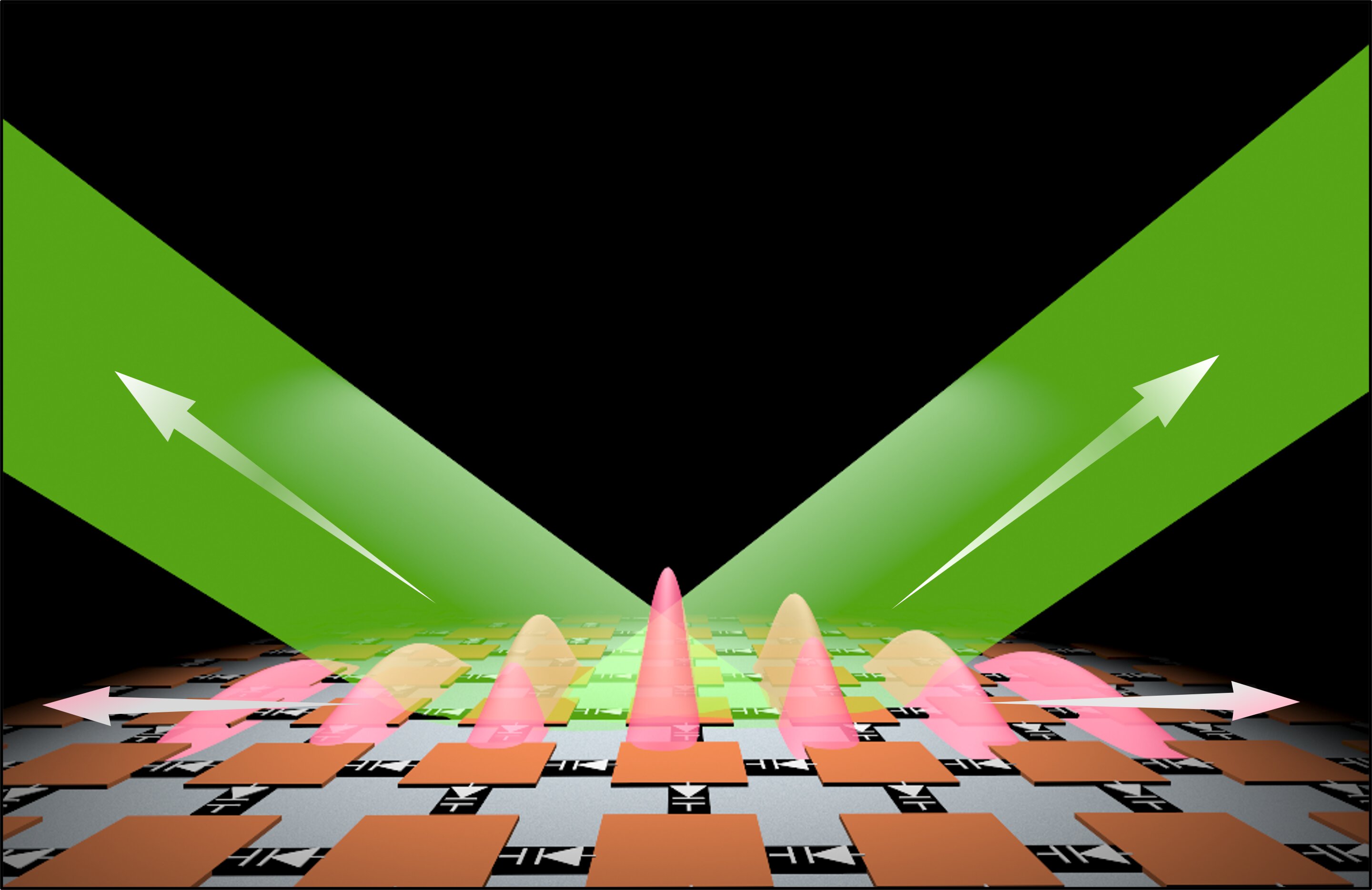
Researchers have created photonic time crystals that operate at microwave frequencies, which can amplify electromagnetic waves. The two-dimensional photonic time crystals have potential applications in wireless communication, integrated circuits, and lasers. The periodic arrangement of photons in the crystal leads to constructive interference and amplification of light, which can boost the efficiency of wireless transmitters and receivers. Coating surfaces with 2D photonic time crystals could also help with signal decay, and the crystals could simplify laser designs by removing the need for bulk mirrors.