Researchers at Johns Hopkins have developed new materials and a process called chemical liquid deposition to create ultra-small, invisible circuits on microchips, potentially revolutionizing the production of smaller, faster, and more affordable electronics in the future.
Researchers at UC Riverside have discovered a method to control electron flow in silicon at the quantum level by manipulating molecular symmetry, enabling nanoscale switches that could revolutionize electronics and energy devices beyond traditional chip limits.
Researchers at the University of Illinois Urbana-Champaign have developed an AI technique that enhances the resolution of Atomic Force Microscopy (AFM), allowing it to visualize material features smaller than the probe’s tip. This breakthrough in nanoscale imaging promises to revolutionize nanoelectronics development and material studies by providing true three-dimensional profiles beyond conventional resolution limits. The deep learning algorithm removes the effects of the probe’s width from AFM microscope images, enabling microscopes to achieve higher resolution in material analysis. This advancement has the potential to significantly improve AFM images and pave the way for further developments in the field.
New research using a van der Waals complex Ar-Kr+ has unveiled insights into electron tunneling dynamics at the sub-nanometer scale, highlighting the crucial influence of neighboring atoms in quantum tunneling. This breakthrough has important implications for quantum physics, nanoelectronics, and the study of complex biomolecules, providing a new way to understand the key role of the Coulomb effect in electron tunneling dynamics and laying a solid research foundation for probing and controlling the tunneling dynamics of complex biomolecules.
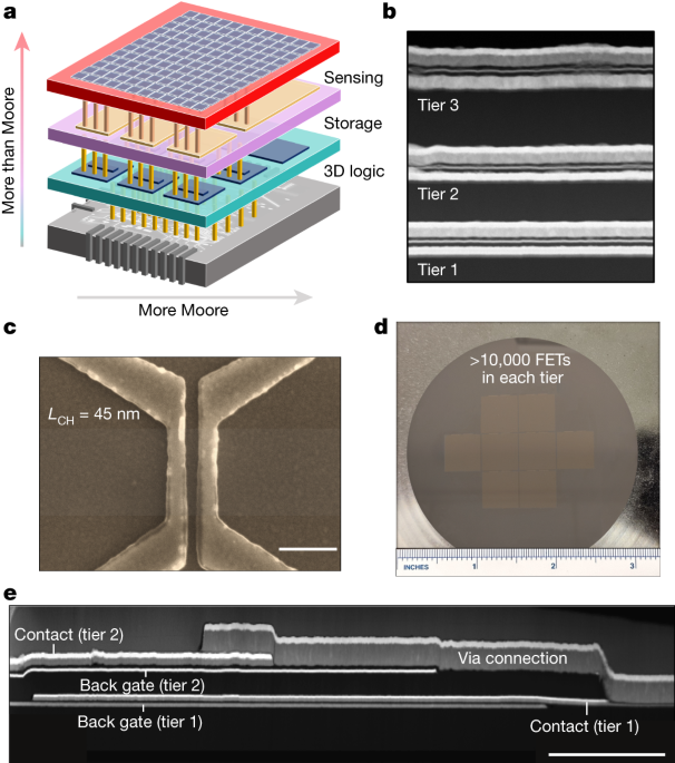
Researchers have achieved a significant advancement in nanoelectronics by integrating two-dimensional field-effect transistors into a three-dimensional structure. This breakthrough paves the way for the development of more efficient and compact electronic devices. The study, conducted at Penn State University, utilized 2D materials such as MoS2 and WSe2 to create the transistors, demonstrating the potential for enhanced performance and scalability in semiconductor technology. The research holds promise for the future of integrated circuits and could lead to innovations in areas such as in-memory computing and flexible electronics.
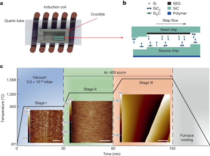
Recent studies have highlighted advancements in the growth and properties of epitaxial graphene on silicon carbide (SiC), which show promise for high-mobility semiconducting applications. The research encompasses the development of graphene with ultrahigh electron mobility, which is crucial for transistor electronics. Techniques such as confinement controlled sublimation and hydrogen intercalation have been employed to produce large area and structured epitaxial graphene, with a focus on understanding and improving the interface structure between graphene and SiC. These advancements could lead to significant improvements in graphene-based nanoelectronics, offering a route to overcome the limitations of low electron mobility typically associated with two-dimensional semiconductors.
Researchers at the University of Colorado Boulder have developed a new technique using doughnut-shaped beams of light to capture detailed images of objects too small to be viewed with traditional microscopes. This method, called ptychography, has previously struggled with highly periodic samples or objects with regularly repeating patterns, such as nanoelectronics. By using beams of extreme ultraviolet light shaped like doughnuts, the researchers were able to collect accurate images of delicate structures as small as 10 to 100 nanometers. This breakthrough could have applications in improving nanoelectronics and inspecting semiconductors for defects without causing damage.
Engineers at Northwestern University have developed a nanoelectronic device that performs machine-learning classification tasks with 100-fold less energy than current technologies. The device can process large amounts of data and perform AI tasks in real time without relying on the cloud for analysis. It is ideal for integration into wearable electronics such as smartwatches and fitness trackers, enabling real-time data processing and near-instant diagnostics. The device was tested on electrocardiogram (ECG) datasets and achieved near 95% accuracy in identifying irregular heartbeats and determining arrhythmia subtypes. The device's tunability, achieved through a mix of materials, allows for dynamic reconfigurability and low energy consumption. The researchers envision these nanoelectronic devices being incorporated into everyday wearables for personalized, real-time applications.
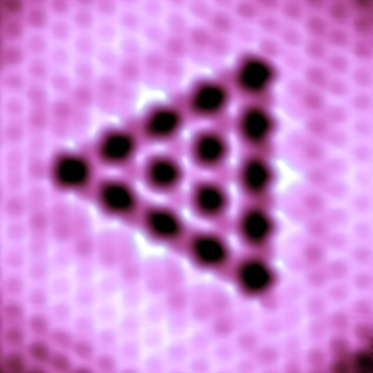
Scientists at the National University of Singapore have achieved a breakthrough in fabricating atomically precise quantum antidots (QAD) using self-assembled single vacancies (SVs) in a two-dimensional transition metal dichalcogenide (TMD). By strategically introducing antidot patterns into carefully designed lattices, they created artificial structures with unique quantum phenomena and transport properties. The QADs, which can be used for quantum information technologies, were fabricated through the self-assembly of SVs into a regular pattern. The structures exhibited robustness against environmental influences and could potentially advance various material technologies.
Scientists at Forschungszentrum Jülich have developed a new type of transistor made from a germanium-tin alloy that has several advantages over conventional silicon-based switching elements. The germanium-tin transistor exhibits an electron mobility that is 2.5 times higher than a comparable transistor made of pure germanium, enabling lower voltages in operation. The transistor is a promising candidate for future low-power, high-performance chips, and possibly also for the development of future quantum computers. The germanium-tin transistor is also a further step towards optical on-chip data transmission.
Researchers at Fudan University and the Shanghai Qi Zhi Institute have proposed a theory of bilayer stacking ferroelectricity (BSF), which could inform the synthesis of 2D ferroelectrics and offer a generalizable guideline of how two stacked layers of the same 2D material can be engineered to exhibit ferroelectricity. The researchers systematically analyzed a series of 2D material groups using group theory, an abstract algebra theory for studying sets of specific objects, to pinpoint the rules underpinning the creation and annihilation of symmetries in bilayer structures, while also identifying possible combinations that would produce BSF. The general theory of bilayer stacking ferroelectricity introduced by the researchers could soon guide new studies aimed at creating bilayer ferroelectrics, facilitating the development of new highly performing devices based on these promising 2D material systems.