Tag

Extreme Ultraviolet Light

All articles tagged with #extreme ultraviolet light

science-and-technology2 years ago

"NASA Engineers Harness Physics to Master Light Focusing"

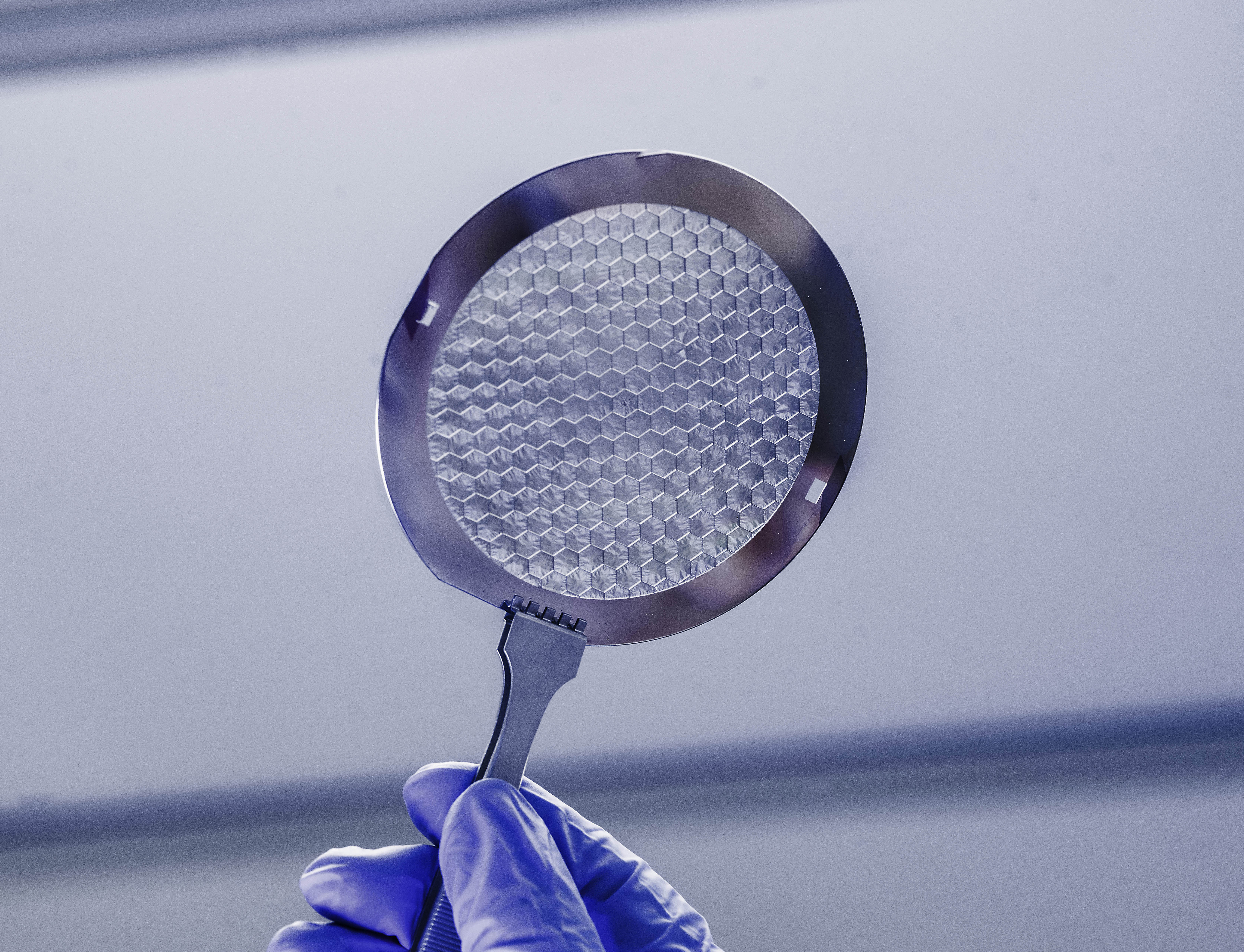
NASA engineers at the Goddard Space Flight Center are pushing the limits of physics to develop photon sieves, a technology that can focus extreme ultraviolet light. These sieves, made from super-thin membranes etched with precise holes, have the potential to capture small-scale features near the surface of the sun that drive the heating and acceleration of solar wind. The engineers have successfully created wider and thinner membranes from materials like silicon and niobium, with the goal of improving light-gathering efficiency. The advancements in photon sieves could lead to more capable space missions and advancements in solar science.

science-and-technology2 years ago

"NASA Engineers Harness Physics to Perfect Light Focusing"

NASA engineers at the Goddard Space Flight Center are developing photon sieves, a technology that can focus extreme ultraviolet light, to capture small-scale features near the surface of the Sun. These sieves, made from super-thin membranes etched with precise holes, can resolve features 10 to 50 times smaller than what can currently be seen. The engineers have successfully produced silicon and niobium sieves, with the latter transmitting up to seven times more light. The technology will be tested in the VISORS CubeSat mission in 2024 and could pave the way for larger future missions.

science-and-technology2 years ago

'Doughnut' beams revolutionize microscopic imaging

Researchers at the University of Colorado Boulder have developed a new technique using doughnut-shaped beams of light to capture detailed images of objects too small to be viewed with traditional microscopes. This method, called ptychography, has previously struggled with highly periodic samples or objects with regularly repeating patterns, such as nanoelectronics. By using beams of extreme ultraviolet light shaped like doughnuts, the researchers were able to collect accurate images of delicate structures as small as 10 to 100 nanometers. This breakthrough could have applications in improving nanoelectronics and inspecting semiconductors for defects without causing damage.