Tag

Semiconductor Devices

All articles tagged with #semiconductor devices

physics2 years ago

"Unifying Forces: The Power of Composite Fermions in Physics"

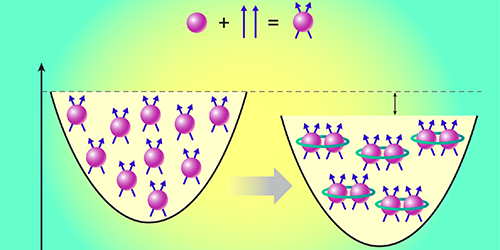
Researchers have developed a new understanding of electron pairing in nanoscale semiconductor devices, leading to the formation of composite fermions and the induction of the fractional quantum Hall effect. This insight could provide clues for the development of high-temperature superconducting materials. The pairing of composite fermions releases an energy that is 20 times more stable than electron pairs responsible for superconductivity in known materials, potentially comparable to the pairing energy seen in the highest-temperature superconductors. Further testing and improvements in device quality are needed to validate these findings, with potential implications for future advancements in materials science and superconductivity.

quantum-physics2 years ago

"Breakthrough: Robust and Ultra-Sensitive Topological Quantum Device Developed by Quantum Physicists"

Quantum physicists from Dresden and Würzburg have developed a semiconductor device made of aluminum-gallium-arsenide that exhibits exceptional robustness and sensitivity due to a topological skin effect, shielding it from external perturbations and enabling unprecedented precision measurements. This breakthrough paves the way for high-precision quantum modules in topological physics and holds potential for applications in the semiconductor industry. The device, measuring about 0.1 millimeters in diameter, demonstrates the topological skin effect at a microscopic scale in a natural semiconductor material for the first time, making it highly suitable for sensor engineering and amplifiers with minuscule diameters.

science-and-technology2 years ago

Atomic-Scale Self-Assembly Revolutionizes Nanotechnology with Light-Trapping Cavities

Researchers have developed a new method for manufacturing semiconductor devices using self-assembly and surface forces. By harnessing the pull-in instabilities between nearby objects, the researchers were able to fabricate nanostructures with few- or sub-nanometer dimensions. They demonstrated the application of this method by creating photonic nanocavities that confine light in air gaps in silicon membranes with aspect ratios exceeding 100. The self-assembled nanocavities exhibited high-quality factors and small mode volumes, surpassing previous experiments on dielectric cavities. The researchers also successfully integrated the self-assembled devices with photonic circuits, demonstrating the scalability and potential for interfacing with top-down planar technology.

technology2 years ago

Canon's Nanoimprint Lithography System Challenges ASML in Semiconductor Manufacturing

Canon has launched the FPA-1200NZ2C nanoimprint semiconductor manufacturing equipment, expanding its lineup to meet the needs of various users. This equipment uses nanoimprint lithography (NIL) technology to transfer circuit patterns by pressing a mask onto the wafer, allowing for faithful reproduction of fine circuit patterns. It enables patterning with a minimum linewidth of 14 nm, equivalent to the 5-nm-node required for advanced logic semiconductors. The new product also features environment control technology to suppress contamination and reduce defects, contributing to the manufacture of cutting-edge semiconductor devices. Additionally, it reduces power consumption and can be used for applications such as metalenses for XR technology.