Atomic-Scale Self-Assembly Revolutionizes Nanotechnology with Light-Trapping Cavities
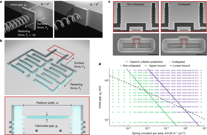
Researchers have developed a new method for manufacturing semiconductor devices using self-assembly and surface forces. By harnessing the pull-in instabilities between nearby objects, the researchers were able to fabricate nanostructures with few- or sub-nanometer dimensions. They demonstrated the application of this method by creating photonic nanocavities that confine light in air gaps in silicon membranes with aspect ratios exceeding 100. The self-assembled nanocavities exhibited high-quality factors and small mode volumes, surpassing previous experiments on dielectric cavities. The researchers also successfully integrated the self-assembled devices with photonic circuits, demonstrating the scalability and potential for interfacing with top-down planar technology.
- Self-assembled photonic cavities with atomic-scale confinement Nature.com
- Bowtie resonators that build themselves bridge the gap between nanoscopic and macroscopic Phys.org
- Revolutionizing Nanotechnology: Photonic Cavities that Self-Assemble at the Atomic Level SciTechDaily
- Self-assembling structures close the gap to trap light Nature.com
- The world's smallest light-trapping silicon cavity Nature.com
Reading Insights
0
9
30 min
vs 31 min read
98%
6,099 → 98 words
Want the full story? Read the original article
Read on Nature.com