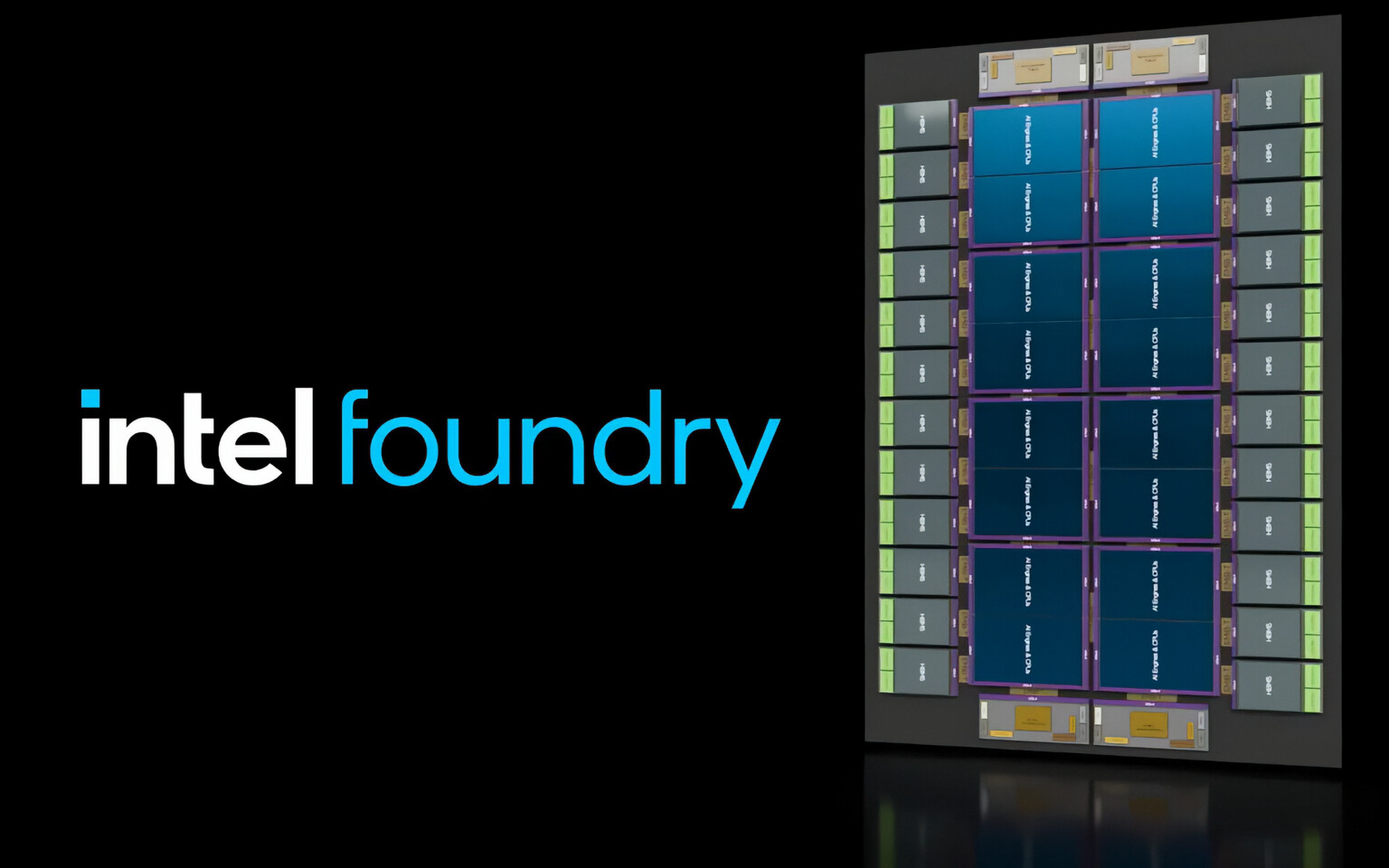
Intel has demonstrated its advanced packaging capabilities, enabling the integration of up to 16 compute dies and 24 HBM5 memory modules in a single package using Foveros 3D and EMIB-T interconnects, leveraging its 18A and 14A process nodes, with plans for high-power GPU designs and competitive positioning against TSMC.
Taiwan's TSMC is considering building advanced chip packaging capacity in Japan, potentially bringing its CoWoS technology to the country, as part of Japan's efforts to revitalize its semiconductor industry. TSMC's plans in Japan include building a plant and establishing a research and development center, with the company partnering with Japanese firms like Sony and Toyota. The move comes amid a global surge in demand for advanced semiconductor packaging, driven by the artificial intelligence boom, and reflects Japan's aim to play a larger role in advanced packaging.
Taiwan Semiconductor Manufacturing Company (TSMC) is reportedly considering building advanced chip packaging capacity in Japan, potentially bringing its chip on wafer on substrate (CoWoS) technology to the country. This move would add momentum to Japan's efforts to revitalize its semiconductor industry, with TSMC already having established operations and partnerships in Japan. The demand for advanced semiconductor packaging has surged globally, and TSMC's potential expansion into Japan aligns with the industry trend.
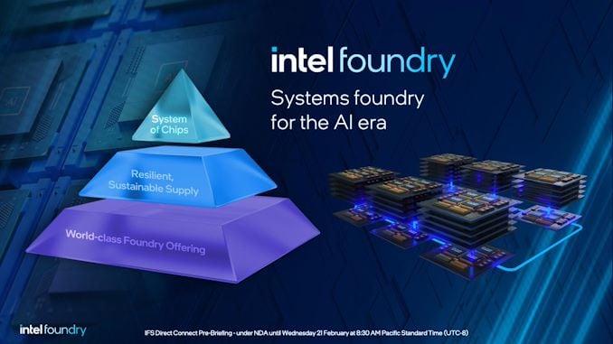
Intel Foundry, formerly known as Intel Foundry Services, is expanding its foundry business with the addition of the 14A process to its roadmap, marking the first extension in over two years. The company is aiming to become a one-stop shop for chip production, offering not only wafer lithography but also advanced packaging, chip assembly, and testing services. Intel is on track to deliver on its promise of 5 nodes in 4 years, with products based on its first EUV-based node, Intel 4, already available in the market. The company is also focusing on collaborating with Electronic Design Automation (EDA) providers and IP vendors to ensure a complete ecosystem for chip design and manufacturing.
Intel has announced the development of industry-leading glass substrates for advanced packaging, which will enable the scaling of transistors in a package and advance Moore's Law. Glass substrates offer superior properties such as ultra-low flatness, better thermal and mechanical stability, and higher interconnect density, making them ideal for high-performance chip packages for data-intensive workloads like AI. Intel plans to deliver complete glass substrate solutions to the market in the second half of this decade, allowing the semiconductor industry to continue scaling beyond 2030.
Intel has announced a breakthrough in the development of glass substrates for chip packaging, aiming to advance Moore's Law. The use of glass substrates will enable Intel to create larger chip packages, allowing for more chips to be fitted into a single electrical package. By the end of the decade, Intel foresees packaging 30 trillion transistors on a glass substrate, along with other innovations such as 3D stacking of chips. Glass substrates offer advantages such as enhanced thermal and mechanical stability, higher interconnect density, and improved power delivery, making them suitable for data-intensive applications like AI. Intel plans to introduce comprehensive glass substrate solutions to the market in the latter half of this decade, ensuring the continuation of Moore's Law beyond 2030.
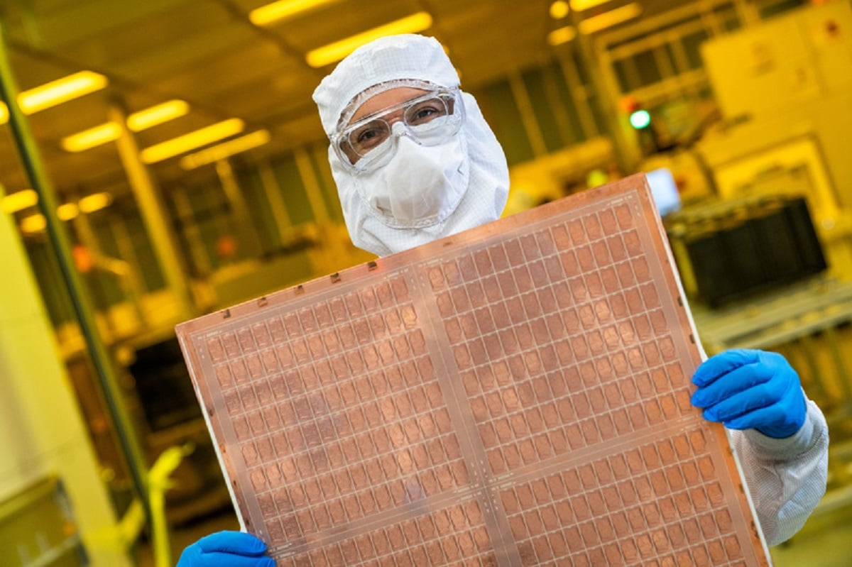
Chiplet technology, a cost-efficient way to package groups of small semiconductors, has emerged as a core part of China's tech strategy as it seeks to achieve self-reliance in semiconductor manufacturing. With the US restricting China's access to advanced machines and materials for chip production, chiplets have become even more important. Chinese authorities have highlighted chiplets in policy documents, and companies like Huawei have actively filed chiplet patents. China's chip packaging industry holds an advantage in chiplet technology, but experts note that the proportion of advanced packaging is still relatively small. Nevertheless, China is rapidly exploiting chiplet technology in various applications, from artificial intelligence to self-driving cars, and major investments in the area are expected.
Chiplets, a way to design chips for higher performance, has become an essential tool for progress in semiconductors. The United States accounts for only 3% of chip packaging, which is overwhelmingly dominated by companies in Asia. The CHIPS Act, a $52 billion subsidy package, aims to reinvigorate domestic chip making by providing money to build more sophisticated factories called “fabs” and stoking advanced packaging factories in the United States to capture more of that essential process. Assembling all the elements required to reduce U.S. dependence on Asian companies is a huge challenge.