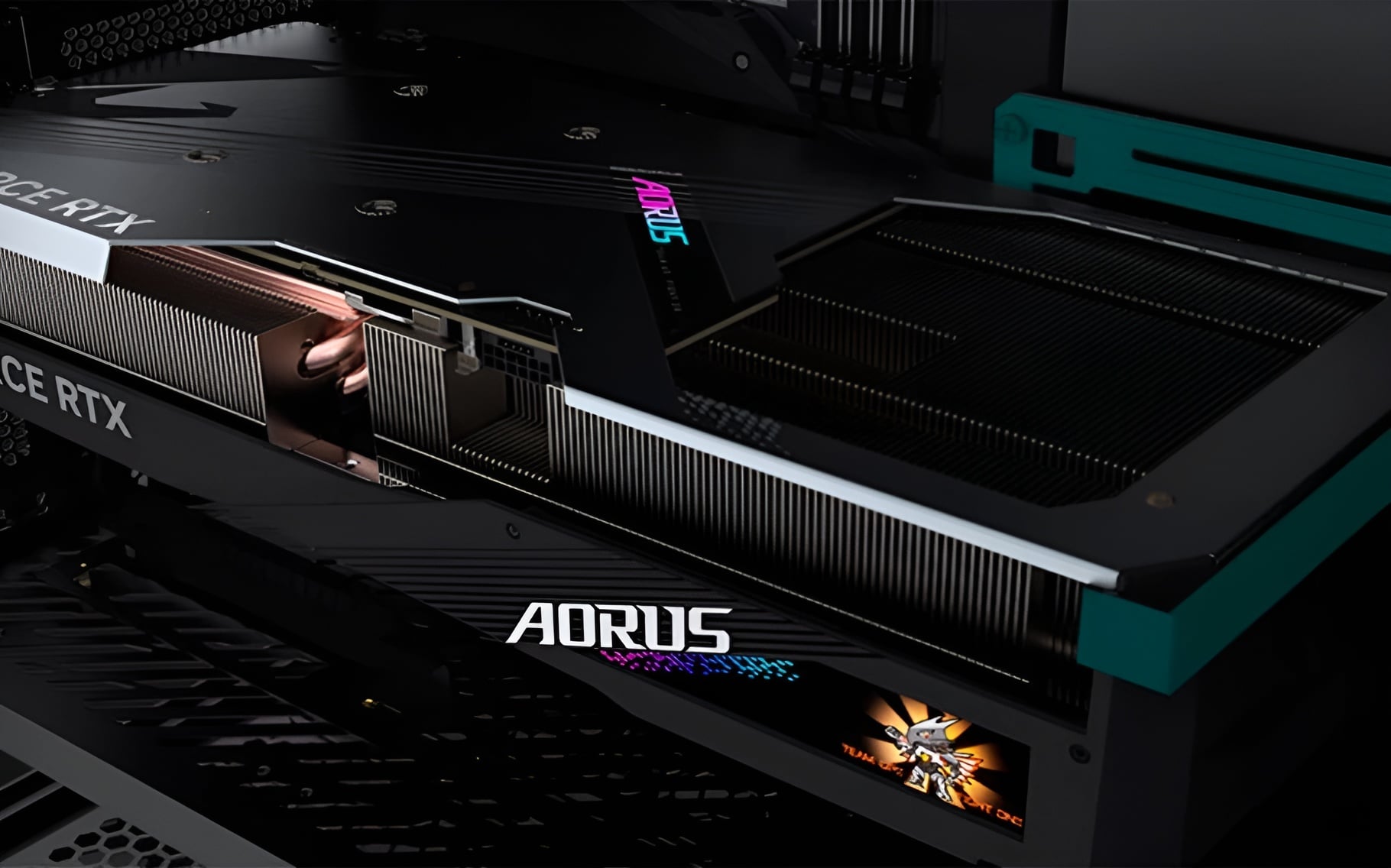
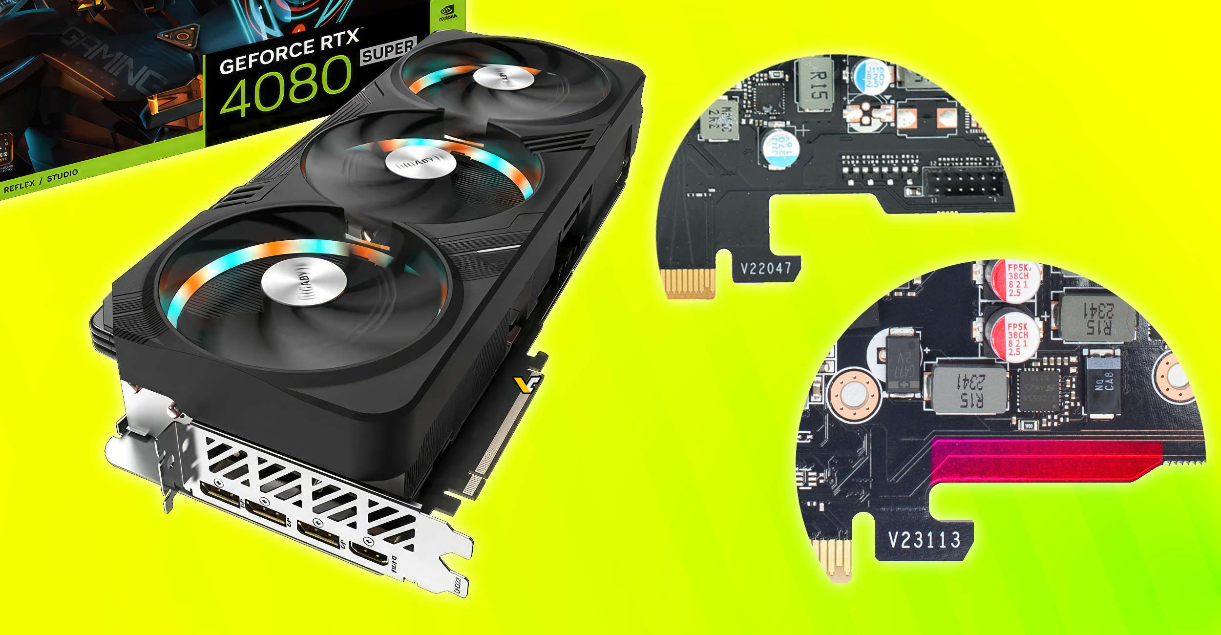
Gigabyte has revised the PCB design of its high-end GeForce RTX 4090 & RTX 4080 GPUs after incidents of PCB cracking surfaced, leading to damaged PCIe lanes and rejected RMA requests. The new "v1.1" batch features a beefier 70a VRM setup, aiming to address the stability and weight distribution issues. While this change may prevent future problems, affected consumers are left without recourse as Gigabyte has not officially acknowledged the issue or confirmed which SKUs have received the design changes.
Gigabyte has updated the PCB design for its RTX 4080/4090 Gaming GPUs to address cracking issues, with the latest revision featuring a stronger PCB around the connector area to reduce the likelihood of cracking. This update comes in response to reports of PCB cracking in some RTX 30 and 40 graphics cards, which could damage signal paths and render the GPU unusable. The design change aims to strengthen the cards and limit potential cracking in the future.
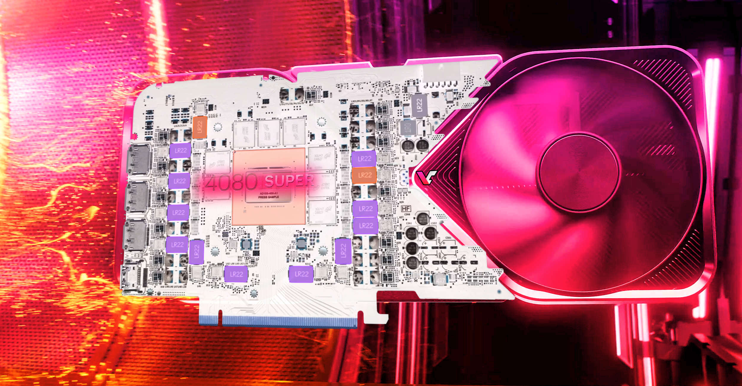
NVIDIA's GeForce RTX 4080 SUPER Founders Edition PCB has fewer power phases than the RTX 4080 non-SUPER, with a reduction from 13 to 11 phases and 3 to 2 memory phases. This change, along with a new color scheme and faster memory, has allowed for lower power consumption during gaming, despite the card featuring a TDP of 320W. Additionally, the GPU codename for the RTX 4080 SUPER is labeled as "PRESS SAMPLE," a departure from previous labeling practices. While these changes are not significant, they offer interesting insights into the design choices made by NVIDIA for their Founders Edition cards.
John Guy has designed a continuity tester that modulates the beeper's tone according to the resistance measured in the circuit, making it easier to track down a short circuit. The circuit is based on a single AD8534 quad op amp chip and features a voltage-controlled oscillator, a comparator with hysteresis, and a low-pass filter. The PCB design is easy to assemble and can be placed in a laser-cut acrylic case, turning it into a neat handheld instrument.