Tag

Optoelectronic Devices

All articles tagged with #optoelectronic devices

nanotechnology1 year ago

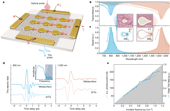
"Nanoscale Vectorial Currents Propelled by Light"

Researchers have developed plasmonic metasurfaces that can control vectorial currents at nanoscale spatial scales and femtosecond timescales. These metasurfaces, consisting of gold nanoantennas on graphene, exhibit strong, light-driven directional responses, with implications for optically controlled and globally varying vectorial photocurrents. The metasurfaces can serve as efficient sources of ultrafast terahertz radiation, including broadband THz vector beams, and can be actively manipulated by incident optical fields or electrostatic gating. The dynamics of the charge flow are studied using electromagnetic, thermodynamic, and hydrodynamic modeling, revealing the potential for spatially varying vectorial current distributions and direct generation of broadband vector beams in the THz frequency range.

science-and-technology2 years ago

"Electron Flow Visualization Inspires Nanoscale Devices with Wing-like Efficiency"

Researchers at the University of California, Riverside have developed a new imaging technique to visualize the flow of electrons around sharp bends in nanoscale devices, similar to how air flows around airplane wings. By designing an "electrofoil" device, the team was able to contort, compress, and expand the streamlines of electric currents, allowing for the measurement of heat generated by electron flow. This research has the potential to improve the design of integrated circuits and optoelectronic devices by identifying areas where heat may cause damage and suggesting the use of gradually curved wires instead of sharp bends.

science-and-technology2 years ago

Revolutionizing Optoelectronic Devices with Atomic-Scale Spin-Optical Lasers

Researchers at the Technion—Israel Institute of Technology have developed a coherent and controllable spin-optical laser based on a single atomic layer. This achievement paves the way for studying coherent spin-dependent phenomena in both classical and quantum regimes, opening new horizons in fundamental research and optoelectronic devices that exploit both electron and photon spins. The laser is constructed using a photonic spin lattice that supports high-Q spin-valley states through the photonic Rashba-type spin splitting of a bound state in the continuum. The researchers used a WS2 monolayer as the gain material, which possesses unique valley pseudospins, enabling active control of spin-optical light sources without the need for magnetic fields.

science-and-technology2 years ago

"Unveiling the Mysteries of Nanoscale Gaps: A Quantum Leap in Understanding"

Scientists at the Center for Functional Nanomaterials (CFN) and the University of Warsaw have created a new layered structure using 2D materials that exhibit unique energy and charge transfer properties. By understanding these material properties, advancements in technologies such as solar cells and optoelectronic devices could be achieved. The researchers used the Quantum Material Press (QPress), a first-of-its-kind experimental tool, to extract, isolate, catalog, and build 2D materials. The QPress creates atomically thin layers and assembles them into heterostructures, which have extraordinary capabilities. By studying these heterostructures, scientists can develop better structures for improved energy absorption, charge transfer, and smaller electronic components.