Scientists have created the world's first quantum semiconductor device using aluminum-gallium-arsenide (AlGaAs), which is safeguarded by a topological quantum phenomenon known as the topological skin effect. This breakthrough development eliminates the need for extremely high levels of material purity, making topological devices increasingly appealing for the semiconductor industry. The device is stable, highly accurate, and can be scaled down to incredibly small sizes, making it suitable for power-intensive applications, sensor engineering, and high-precision sensors and amplifiers. The success was achieved through innovative experimentation and sustained collaboration among scientists at different locations.
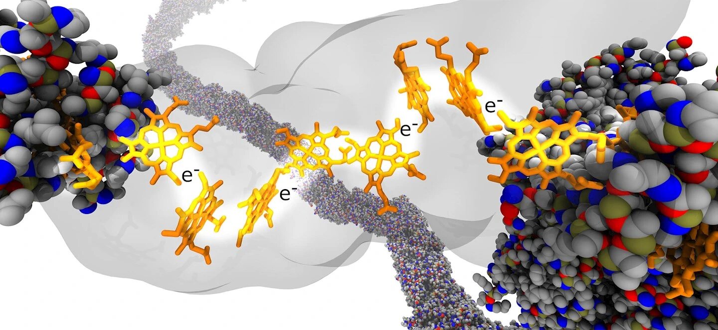
Researchers have used computer simulations to study the movement of electrons through biological nanowires made of proteins. By manipulating variables such as the length and thickness of the nanowires, they discovered that electron transport depends on the motion of the proteins within the wire. Understanding how to optimize electron flow in biological nanowires is crucial for potential applications in connecting biological processes to conventional electronics.
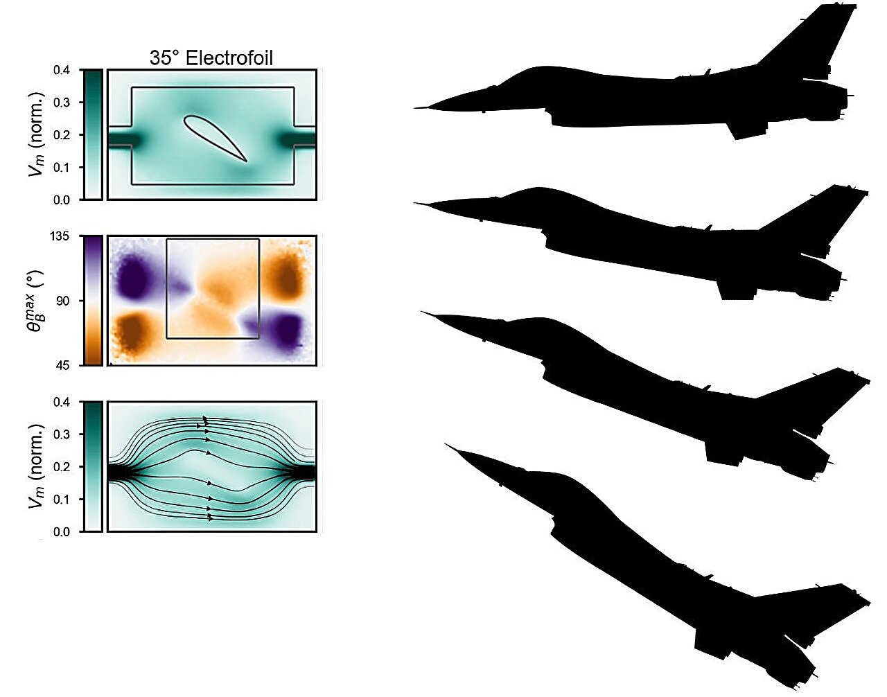
Researchers at the University of California, Riverside have developed a new imaging technique to visualize the flow of electrons around sharp bends in nanoscale devices, similar to how air flows around airplane wings. By designing an "electrofoil" device, the team was able to contort, compress, and expand the streamlines of electric currents, allowing for the measurement of heat generated by electron flow. This research has the potential to improve the design of integrated circuits and optoelectronic devices by identifying areas where heat may cause damage and suggesting the use of gradually curved wires instead of sharp bends.