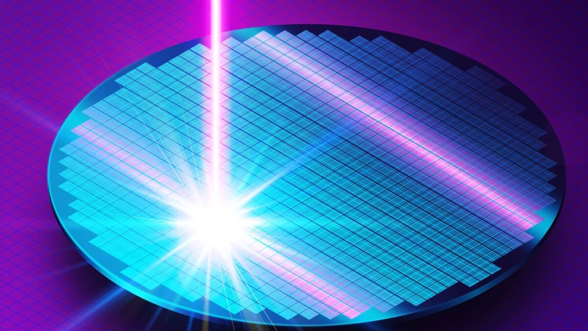
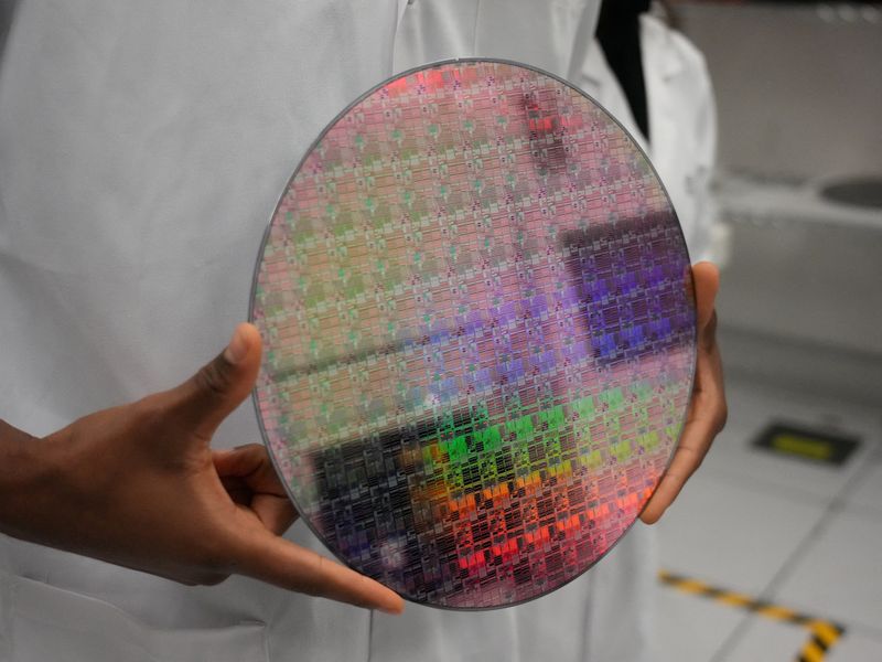
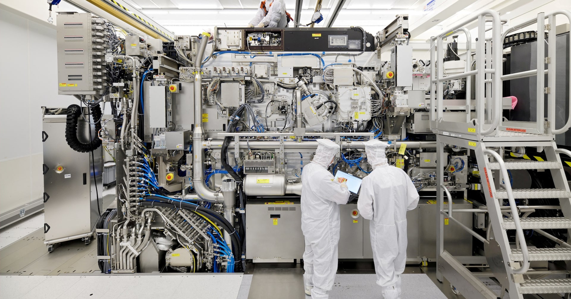
The article explores the significance of ASML's $400 million EUV lithography machine, essential for GPU manufacturing and AI development, highlighting its complex technology, geopolitical implications, and the inevitable progression towards more advanced and expensive machines, reflecting on the fleeting nature of technological dominance.
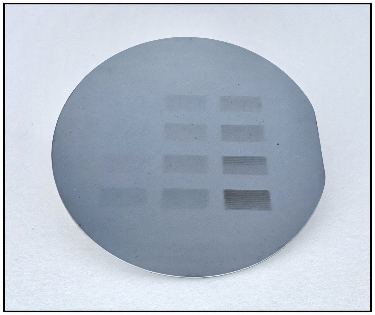
Substrate, a US startup, claims to have developed a new chipmaking tool using X-ray lithography that can rival ASML's advanced EUV equipment, aiming to reduce costs and boost US competitiveness in semiconductor manufacturing, with potential national security implications.
Johns Hopkins researchers have developed a new, precise, and cost-effective process using advanced B-EUV lithography and novel metal-organic resists to create microchips with circuits so small they are invisible to the naked eye, potentially enabling smaller, faster, and more affordable electronics in the future.
ASML, the largest supplier of equipment to computer chip makers, reported weaker than expected first-quarter new bookings, with sales to China holding up despite U.S.-led restrictions. The company is seeing a lull in demand for its most advanced machines but is gearing up for strong growth in 2025 due to strong demand for AI and memory chips. Despite the weak bookings, ASML still expects a stronger second half of the year and describes 2024 as a "transition year". Sales of ASML's lithography systems to customers in China made up a record 49% of the total in the first quarter, and the company is set to benefit from new chip plants planned with support from governments in various countries.
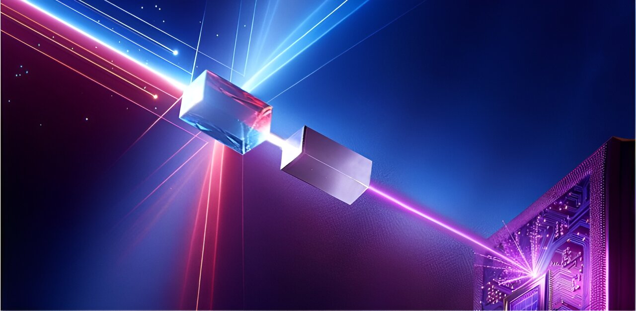
Researchers at the Chinese Academy of Sciences have achieved a significant breakthrough in deep ultraviolet (DUV) laser technology by generating a high-power, narrow linewidth solid-state DUV laser at 193 nm using a two-stage sum frequency generation process employing LBO crystals. This innovation, known as the "hybrid ArF excimer laser," offers enhanced coherence and narrow linewidth, leading to improved performance in high-throughput interference lithography and direct processing of various materials with minimal thermal impact. The research not only pushes the boundaries of DUV laser technology but also holds promise for revolutionizing applications across scientific and industrial domains.
Canon, known for its cameras and printers, has launched a new "nanoimprint lithography" system called FPA-1200NZ2C, which it claims can manufacture semiconductors equivalent to a 5nm process and go as small as 2nm. This puts Canon in direct competition with Dutch firm ASML, which dominates the extreme ultraviolet (EUV) lithography machine space. ASML's machines are crucial for manufacturing the most advanced chips, and its EUV technology has become popular among chipmakers. Canon's machine does not require a special wavelength light source, reducing power consumption. The development of Canon's nanoimprint lithography technology comes at a time when the global demand for chips is increasing, and geopolitics surrounding semiconductor supply chains are intensifying.
Chinese chipmaking machine suppliers, including Shanghai Micro Electronics Equipment Group, saw a surge in stock prices after reports of a significant technological breakthrough by a state-backed firm. The breakthrough raises hopes that China can reduce its reliance on US semiconductor techniques. The Shanghai firm is working on delivering its first system based on 28-nanometer technology, a crucial component for making silicon used in various products. China has been pushing for the development of local technologies in strategic sectors, including chipmaking, to counter US restrictions. However, it remains uncertain if the Shanghai firm can produce these machines in large quantities.