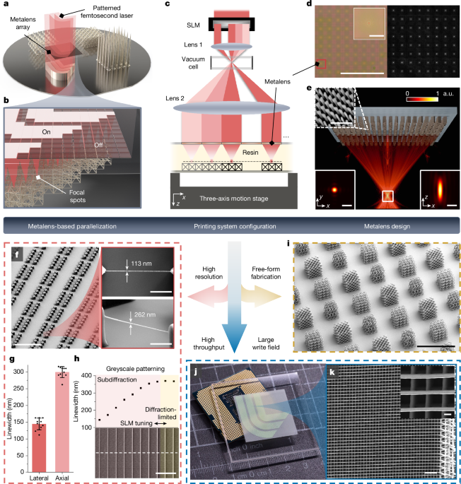
The article discusses advanced 3D nanolithography techniques utilizing metalens arrays and spatially adaptive illumination to achieve high-resolution, complex microstructures, highlighting innovations in optical fabrication methods and their potential applications.
Researchers led by Associate Professor Niels Quack from the University of Sydney have developed a microfabrication process that combines optics and micro-electro mechanical systems (MEMS) in a microchip, enabling the creation of devices like micro-3D cameras and gas sensors for precision air quality measurement. The technology uses semiconductor manufacturing techniques to create a new, more energy-efficient generation of devices for fiber-optical communications, sensors, and even future quantum computers. The photonic MEMS are compact, consume very little power, are fast, support a broad range of optical carrier signals, and have low optical loss.