Direct imaging of sub-moiré electrostatics with an atomic single-electron transistor
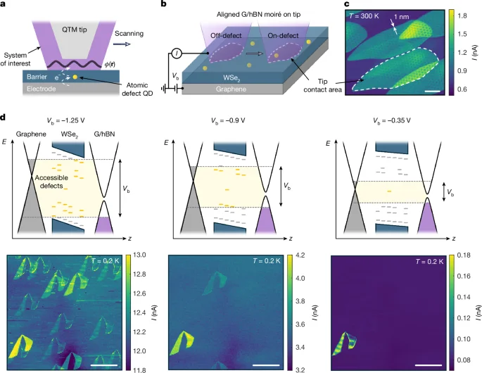
A new scanning probe, the atomic single-electron transistor (SET) built on the quantum twisting microscope, uses a single atomic defect as a sensitive quantum dot to map the local electrostatic moiré potential at a graphene/hBN interface with ~1 nm resolution and sensitivity to a few parts per million of an electron charge. By tracking shifts in the defect’s Coulomb blockade peak as the tip scans, the authors obtain direct 2D maps ϕ(x,y) of the moiré potential, observing a large ~60 mV peak-to-peak amplitude with approximate C6 symmetry that is only weakly dependent on carrier density. The measurements, performed across moiré unit cells at multiple fillings, reveal equipotential rings that expand with gate bias. Comparison with theory shows that self-consistent screening by graphene largely preserves pseudopotential shapes but reduces magnitude; the two leading terms nearly cancel to yield near-C6 symmetry, yet the observed amplitude is about twice the theoretical prediction, indicating gaps in current understanding. The atomic SET’s extreme spatial and potential sensitivity enables detailed studies of charge order, symmetry-broken phases, and exotic quasiparticles in a wide range of quantum materials, with the potential to image thermodynamic properties and phenomena at scales below the Fermi wavelength and moiré lengths.
Reading Insights
1
10
31 min
vs 33 min read
97%
6,466 → 198 words
Want the full story? Read the original article
Read on Nature